
Advanced Circuit Board Design — 5-Day Training Course
$5500.00
Advanced Circuit Board Design
5-Day Training Course Outline
Course Overview
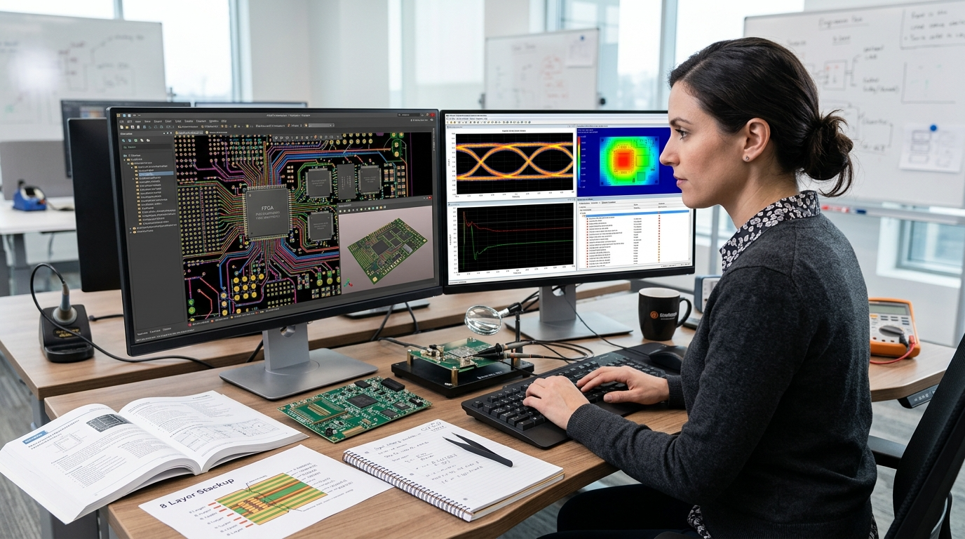
The Advanced Circuit Board Design training course is a fast-track, five-day programme for experienced PCB designers and hardware engineers ready to move beyond the basics. Covering high-density interconnect (HDI), signal integrity (SI), power integrity (PI), controlled impedance routing, EMI/EMC mitigation, thermal management, and Design for Manufacturability (DFM), this course bridges the gap between functional PCB layouts and production-ready, high-performance board designs.
Delivered through structured lectures, EDA tool demonstrations, and hands-on design exercises using industry-standard tools (Altium Designer, Cadence Allegro, or Mentor Graphics), participants leave with immediately applicable skills for high-speed digital, mixed-signal, RF, automotive, aerospace, IoT, and 5G electronic products.
Who Should Attend: Mid-to-senior PCB layout designers, hardware and signal integrity engineers, embedded systems developers, RF designers, and engineering leads responsible for board-level product quality and first-pass success.
Prerequisite: Working knowledge of PCB design fundamentals — schematic capture, basic layer stackup, standard component footprints, and familiarity with an EDA tool environment.
🎯 Learning Objectives
Upon completion, participants will be able to:
Design multi-layer stackups optimised for signal integrity and EMC compliance
Apply controlled impedance routing for high-speed single-ended and differential signals
Implement robust power distribution networks (PDN) with effective decoupling strategies
Execute advanced via techniques including back-drilling, blind/buried, and via-in-pad
Route complex BGA fanout patterns and fine-pitch HDI designs with microvias
Apply EMI/EMC suppression techniques to reduce test failures and redesign cycles
Perform pre- and post-layout SI/PI simulation and interpret eye diagrams and S-parameters
Deliver fully DFM-compliant design packages ready for volume manufacturing
📅 5-Day Course Structure
Day 1 — Stackup Design, Materials & HDI Architecture
Session 1 — Advanced Multi-Layer Stackup Design
High-speed design fundamentals: transmission line theory, signal propagation, and dielectric constants
Core vs. prepreg layer construction and material selection (FR4, Rogers, Megtron 6, PTFE)
Layer count optimisation for SI, PI, and EMC performance
Symmetric vs. asymmetric stackups — warpage risk and mitigation
Embedded passive materials and HDI-specific laminate considerations
IPC-2221, IPC-2222, IPC-4101 material specifications overview
Session 2 — HDI & Microvia Design
What is HDI? — class types per IPC-2226, design density drivers
Microvia formation: laser-drilled blind vias, buried vias, and stacked/staggered configurations
Sequential lamination fabrication processes and their design implications
BGA fanout strategies on HDI boards — escape routing for fine-pitch area array packages
Circuit compression and non-orthogonal placement for reduced board area
Embedded active and passive components: cavity design and IPC-2316/IPC-6017 compliance
Hands-on Exercise: Layer stackup planning and HDI via structure definition for a multi-layer reference board
Day 2 — Signal Integrity & Controlled Impedance Routing
Session 1 — Signal Integrity Fundamentals
Signal degradation mechanisms: reflections, ringing, overshoot/undershoot, and jitter
Transmission line behaviour — characteristic impedance, termination topologies (series, parallel, Thevenin, AC)
Crosstalk: near-end (NEXT) and far-end (FEXT) — trace separation rules and guard routing
Eye diagrams and S-parameters — interpreting simulation output for design decisions
Rise time, fall time, and the knee frequency — determining when SI rules apply
Session 2 — Controlled Impedance & Differential Pair Routing
Single-ended controlled impedance: microstrip and stripline calculations
Differential pair routing: length matching, skew control, spacing symmetry, and common-mode noise
High-speed interfaces in practice — USB 3.x, HDMI, PCIe Gen 3/4, LVDS, MIPI, and DDR4/5
Routing over splits and voids — return current path disruption and mitigation
EDA constraint-driven routing: setting SI rules, length tuning, and timing budgets in Altium/Cadence
Hands-on Exercise: Controlled impedance trace calculation and differential pair routing exercise (PCIe / USB scenario)
Day 3 — Power Integrity, Via Design & EMI/EMC
Session 1 — Power Distribution Network (PDN) & Power Integrity
PDN modelling: target impedance, plane resonance, and loop inductance
Decoupling capacitor selection, placement strategy, and self-resonant frequency
Bulk, mid-frequency, and high-frequency decoupling — a layered approach
Plane splits, anti-pad design, and power island strategy for mixed-voltage boards
Power integrity for FPGAs, high-speed processors, and DDR memory interfaces
Simulation: PDN impedance analysis and power rail collapse prevention
Session 2 — Via Optimisation & EMI/EMC Design
Via types: PTH, microvia, blind, buried, and via-in-pad — current capacity and thermal behaviour
Via stubs, back-drilling, and their impact on high-frequency signal integrity
EMI radiation sources: differential-mode and common-mode emissions
EMC layout strategies: slot minimisation, stitching capacitors, guard rings, and shielding
Filter placement, ferrite beads, and TVS/ESD protection routing
Compliance frameworks: CISPR, FCC Part 15, IEC 61000 — design-phase impact reduction
Hands-on Exercise: PDN decoupling layout review + EMI/EMC stackup and routing audit exercise
Day 4 — Thermal Management, DFM & High-Speed Constraints
Session 1 — Thermal Management & High-Power Design
Power dissipation analysis: identifying hotspots in high-current and high-frequency layouts
Thermal via arrays — design rules, voiding prevention, and IPC-2152 current carrying capacity
Copper pour strategy: solid fills, hatched fills, and heat spreading plane design
Thermal interface materials, heat sink mounting footprints, and keep-out zone planning
Thermal simulation integration — using EDA thermal tools and interpreting results
Case applications: DC/DC converter boards, motor drivers, RF power amplifiers
Session 2 — Design for Manufacturability (DFM) & Design for Test (DFT)
DFM fundamentals: pad and via sizing tolerances, annular ring requirements, clearance rules
Soldermask and silkscreen design — aperture rules, tenting, and registration tolerances
Panelisation strategies: V-score, tab routing, fiducials, and assembly yield optimisation
Design for Test (DFT): test point placement, boundary scan (JTAG), and ICT probe access
Generating complete manufacturing output packages: Gerber RS-274X, ODB++, IPC-2581, NC drill, BOM, and pick-and-place files
DFM check workflow within EDA tools — automated rule verification before release
Hands-on Exercise: DFM audit on a sample board — identifying and correcting manufacturing constraint violations
Day 5 — Simulation, Validation & Capstone Project
Session 1 — SI/PI Simulation & Post-Layout Verification
Pre-layout SI planning: topology selection and material/stackup impact modelling
Post-layout SI simulation workflow: extracting parasitics, running SPICE/IBIS models
3D field solvers — when to use and how to interpret results (Ansys HFSS, HyperLynx)
PI simulation: AC impedance sweeps and decoupling network validation
EMC simulation: near-field scanning and coupling path identification
Real-world validation: comparing simulation to measurement (TDR, VNA, oscilloscope)
Session 2 — Capstone Review, Assessment & Course Wrap-Up
Participant design project review and peer critique session
Common advanced PCB design failure modes — lessons from production case studies
Emerging technologies: chiplets, SiP (System-in-Package), embedded RF, and 3D PCB structures
Industry standards recap: IPC-2221, IPC-2226, IPC-2316, IPC-6012, J-STD-001, IPC-A-610
Written assessment and certificate of completion award
Individual feedback, Q&A, and next-steps guidance
📜 Course Summary
Detail | Information |
|---|---|
Duration | 5 Days (classroom or live-virtual) |
Format | Lecture + EDA Tool Demos + Hands-on Labs |
Level | Advanced — experienced PCB designers/engineers |
Tools Referenced | Altium Designer, Cadence Allegro, Mentor Graphics |
Standards Covered | IPC-2221, IPC-2226, IPC-2316, IPC-4101, IPC-6012, IPC-2152, J-STD-001 |
Assessment | Design exercises + written assessment |
Certificate | Certificate of Completion awarded on pass |
🔗 Complementary Courses & Standards
IPC-A-610 CIS — Acceptability of Electronic Assemblies
J-STD-001 CIS — Soldering Requirements for Electronic Assemblies
IPC-7711/7721 CIS — Rework, Modification & Repair of Electronic Assemblies
Signal Integrity & EMC for Hardware Engineers (advanced follow-on)
Course content aligned with current IPC design standards and industry best practices for high-speed, high-density PCB development. Tool-specific exercises can be tailored to the EDA platform used by your organisation. IPC Electronics U | Datastat Advanced PCB & SI Course | EMA DFM Training